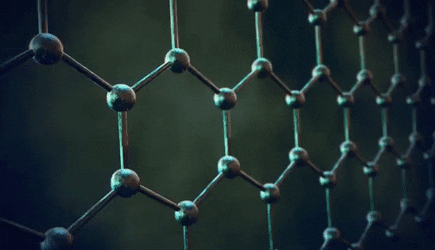
-Overview of possibleGraphene applications-

Mechanical properties
Graphene combines the peculiarity of being a materialextremely light (a density of 0.77 mg / m² is estimated)with exceptional mechanical resistance properties (it is estimateda breaking load of around 42 N / m and Young's modulusaround 1 TPa).The resistance measures comemade with the AFM (diamond tip).Membrane membranes are suspendedgraphene on top of the micro-holes onSiO2 substrate; the membranes inactually they join in partvertically to the walls (2-10 nm).Repeatable and without data are obtainedhysteresis, which demonstrates the factthat the membranes do not slip.Deformation and rupture take placein the limited area below thetip.
Application fields
Application fieldsDespite the graphene is relatively easy to prepare inlarge quantities and properties theorized or measured on a scalemicroscopic are excellent, it is very complex to translateall this in results on a macroscopic scale. This is because inall in all, nanostructures and i must be combined with each otherweaker bonds and defects limit the properties of the materialthe final. The most direct method of obtaining this, already usedalso for other nanoscopic structures, it is the packing ininorganic sheets, ie the so-called graphene paper. Another onepossibility is to exploit the dispersion in a means to createof composite materials that improve or change propertiesof the matrix.An alternative field of application that limits the problemit consists in finding applications directly on a scalemicroscopic. In this case the practical outcomes are limited by the factthat these are still applications at the beginning and not very definedlike the NEMS.
The material that is obtained is rather homogeneous and has strong bondsbetween the layers: this can be deduced from the rigid response under load and from theflat fracture surfaces.Oxidized graphite can becompletely exfoliated in water: inin this way a suspension is obtainedcolloidal of GO large about 1μm.These can be depositedby vacuum filtration, like thisto obtain a dark sheet havingmicrometric thickness. Measures ofX-diffraction reveal: that the layersthey are packaged with distances of 0.83nm due to molecular layers ofwater, and that the packing is orderedinvolves an average of 6-7 layers of
Oxidized graphene paper
Subjected to load tests it is determinedan elastic modulus on average around32GPa, also reinforces after the first onesloading / unloading cycles (alignment of thefibers as in similar materials).In bending tests it has a roleimportant is the water present between the layersthat is pushed away near thedefects provoking the delamination of thelayers from disconnected areas.
Ultimately, the material demonstrates onemechanical resistance higher than thatof carbon based sheets (graphite orbuckypaper). It is obtained at low costand this would allow the use of sheets withlarge surfaces for membranes,supercapacitors, ion conductors, etc
Graphene card
One of the limitations of the previous materialis that the GO does not have the propertiesconductive graphene. It is notpassable the way to reduce afollowing the GO-paper throughannealing because they get worsemechanical properties. However it ispossible to reduce the GO in suspensionby hydrazine. In doing so it is notas much as possible to redisplay the graphene inwater because hydrophobic, and you get asheet with similar structure but withmetallic shine. The spacing betweenfloors are reduced to 0.39 nm (slightlygreater than in graphite).
Graphene card
The mechanical properties are similaror slightly higher than those of theGO-paper, with the difference thatthe latter worsens very quicklyif heated at high temperatures. Thebehavior under load tends tobe less plastic afterwardsof annealing: until you reach themaximum modulus of elasticity around the42 GPa for heating at 220 ° C.Also the conductivity increases with ihigh temperature treatments: we passfrom 11800 S / m to 220 ° C up to 35100 a500 ° C.Finally, studies on thebiocompatibility of the material, which it isrevealed to be a good substrate for thecell growth.
Composite materials
A mechanism commonly used to improve thetoughness of polymeric or ceramic materials consistsincorporating particles and fibers into the main matrixanother material, obtaining a reinforced composite.The fracture toughness of the materialdeparture improves, because in the casein which in the matrix under stress yescreate cracks, thesemeeting the dispersed phase moreresistant they would not be able topropagate (crack impeding) ormeeting the interface would comediverted from the propagation directiondamping their energy (crackdeflection). In general, an increaseof the area affected by the fractureabsorbs energy, delaying breakage.
Reinforced composites
Methods for the production of layers ofpartially oxidized graphene, canbe conveniently used foruse in composites, given the ease withwhich, these, can be dispersed inpolar solvents. Being able to get onegood dispersion in bisphenol-A is themain limit: competitive mechanismagglomeration limits the potential.There is also an increase in the Tg.
Fracture toughness increases by 65% by charging oneepoxy resin with only 0.125% ingraphene mass (compared to 0.5% CNT or 15% fillersconventional SiO2 type to obtain increments anywaylower).This wide difference is related to greater efficiencyin the mechanism of deflection of the cracks due to thetwo-dimensionality of graphene.
Conductive composites
Another possibility exploited in the field of composites is thatto obtain polymeric materials capable of conducting heat and / orelectricity. This becomes possible if the system reaches thepercolation threshold since the polymer matrix is insulating.We always start from oxidized graphite,for the possibility of dispersion,however we must keep theconductivity. The problem is solvedfunctionalizing with isocyanates. Inthis way it can be dispersed in DMFto reduce the GO in solutiontogether with styrenic polymers (PS,ABS, BS tires) that neprevent agglomeration.Next steps allow theprecipitation of the composite fromsolvent and hot molding.
Conductive composites
The percolation threshold of thecomposite polystyrene-graphene isaround 0.1% by volume (σfollows a power law).Loaded at 2.5% by volume, yesit already has a conductivityof the order of 1 S / m.The threshold is similar or somehigher than thoseof composites with SWNT and thesimilar conductivity.
Main advantages compared to SWNTs as fillers (in addition toimprovement of mechanical, rheological andchemical stability, thanks to the larger exposed surface of thegraphene), are the lower costs of production and the possibility ofapplication on an industrial scale.
NEMS nano electromechanical systems
The miniaturization of mechanical devices is one of the frontiersmore revolutionary. The simplest conceivable prototype is aactuator that converts energy (thermal, electromagnetic,electrical, chemical) of an external stimulus in mechanical energy.Scale resonators have been studiednanometer. One (or more) plan ofgraphene placed above an incision in aSiO2 substrate remains blocked forinteractions of VdW. It is possible to excite imodes of vibration of graphene both with aelectric signal that optical in frequency, inboth cases the answer is checkedby deflecting a laser.Two possible applications are thedetermination of ultra-small massesor of ultra-weak forces (in the casetreated with sensitivity of 0.9 fN / Hz).
NEMS: microactuators
With photolithographic techniques it is possiblemake a microactuator. This isconsisting of a structured hybrid cantileverin epoxy with a resistance of abovegraphene (50-60 kΩ). When the serpentineis fed there is a heating that yestransmits to the epoxy film, given thedifferent expansion coefficientthermal of the two materials, there is oneactuator deflection.Deflection is linear to growof temperature and electric power(proportionality is not direct because there isan initial deformation)
The device is transparent, has times ofrapid response (tens of μm / s), canoperate in frequency, and act both asactuator that as a detector.
Thermal conduction properties
Carbon nanostructures generally report high values of thermal conductivity (SWNT ~ 3500 W / mK, MWNT ~ 3000 W / mK) that exceed the best crystalline material (diamond 2200W / mK). For graphene the measured value is even higher: 5300 W / mK. The measure of this property is particularly complex. The heating is done with a laser in the central area of graphene, suspended above the incision, so that the heat is propagate along the plane. Side layers of graphite serve to dissipate heat into excess, given that the coupling thermal with SiO2 would be negligible. The measurements are made by confocal Raman spectroscopy, since the ω of the peak G varies according to the temperature. In a similar way the intensity of the peak is established power actually absorbed.
Heat sinks
Graphene could contribute to electronics, less revolutionary but nevertheless promising, in terms of heat dissipation in electronic devices. The problem of overheating it tends to get worse as it shrinks dimensions of the circuits, because it becomes difficult to exchange heat in structures of increasing complexity and yes create hot-spots. Once rendered possible integration of graphene in microelectronics, his two-dimensional geometry it would facilitate the development of guides thermal and could be coupled with such materials nanotubes or synthetic diamond in the case it should be electrically isolated.
Optical properties: transparent contacts
Absorbance for a single plane ofgraphene is 2.3% (contributions fromreflection is negligible <0.1%)practically independent of thewavelength of light in thespectrum 300-2500 nm.This, combined with the low resistivity, themake it an ideal candidate for contactstransparent (replacing the expensiveITO). In addition to low cost, the advantagescompared to ITO are: conductivitycomparable (exceeds ITO if drugged instable way) but bettertransmission and no absorptionaround 4 eV, less chemical fragility emechanical with the possibility of use inflexible devices.
Optical applications
Photovoltaics:Immediate benefits in low-cost cells(organic, DSSC, etc.) not just for useas a contact, but also to improve thecharge transport or as catalyst alplace of Pt in the DSSC (η cala from 6.3% to4.5% with the rest of the rest).LED:Exploitable as a flexible contact forOLED. It also eliminates the problems created by thespread of In and the contaminations dueto metal contacts, which shorten lifeof the organic device.photodetectors:Having a broad absorption band(from UV to THz), it would be possible to dowide-spectrum detectors and given the highmobility would have response timesvery high compared to the current ones.
Optical applications
Touch sensitive screens:In those capacitive mechanical stress is reduced,resistive ones work fordeformation by contacting two electrodes.Limitations of costs, fragility / duration and resistancechemistry for ITO.Smart windows:Thermotropic LCs dispersed in a polymer inabsence of field diffuse light (windowopaque), with the orientation following the field ilmaterial becomes transparent. Replace theexpensive ITO would create market appeal.Non-linear optics:Applications as a saturable absorber forlaser. It has the advantage of broadband (notuning), speed of response and is easilycan be integrated into appliances once it has been put ona polymeric sheet.
Sensors
Devices that after an external stimulus change the own state and by the variation of their property measurable, allow the interpretation of a signal.
You can distinguish a priori depending on the fields ofapplication: physical, chemical and biological sensors
In general great variability in mechanisms of operation and in type of signal supplied output.
Chemical and biological sensors
This category of sensors is used for measurements of concentration of a chemical species. Generally, the analyte is found in the gas phase or in solution. The latter case is obligatory as regards biological sensors, since the recognition of the analyte takes place by means of substances biological.
Chemical and biological sensors
They are therefore made up of a part of the active device whichmust react to changes in the analyte concentration frommeasure and a part, passive, which acts as a transducerof the response in an easily acquired signal (inseveral cases are acquired electrical signals, so they canthere are later stages of amplification, conversion, etc.).
Transduction
Depending on the mechanism transduction can be subdivided into four classes main:
● thermal (use the ΔH of reaction with the material sensitive)
● mass (microbalance piezoelectric for determine the accumulation)
● electrochemical (variations conductivity in transistors)
● optical (fluorescence, chemiluminescence, etc. greater complexity but strong selectivity)
Requests and compromises
Extremely important for sensor operationare the selectivity (generally high for the biologicals) and thereversibility. To achieve this it is required that the interactionbetween analyte molecules and the chemically active material of thesensor is not too intense and is possiblyspecific.Another parameter that strongly conditions the field ofapplicability of a sensor is its robustness (mechanical,thermal, but above all chemical).Ideally, therefore, it is required that a chemical sensor has:
● high sensitivity
● wide dynamic
● specific response for the analyte
● rapid response and recovery times and long-term stabilityterm
Graphene as a sensitive material
Various properties of graphene canbe interesting to meet theprevious requests: chemical stabilityhigh of the 2D lattice (unlikeCNT, local faults affect littletransport and mechanical properties),but also possibility offunctionalization (to improve thespecificity of the answer).It makes it possible to strongly vary thenumber of carriers, both electrons andgaps, depending on the chemical speciesadsorbed on the surface: effect ofdoping at the base of sensors asemiconductors.
Graphene as a sensitive material
Electronic and mechanical properties favorable forimplement transduction mechanisms (eg contactselectric, transistor, etc.):
● high mobility (quick response),
● large area available (exposure is maximum, likeadsorption),
● high conductivity and rare defects (they contribute to reducing thenoise and improves SNR)
● possibility of ohmic contacts (use with various transducers).Possibility of application also in physical sensors.Greater simplicity and lower production costs of graphene(or its oxidized forms later reduced) respectto the CNTs.
Semiconductor sensors
Application as gas sensors.The operating principle isbased on charge transferfrom the moleculesof the analyte and requires thata chemisortion occurs on thesemiconductor surface.
The mechanism is redox: there may be agentsreducing agents (electron donors) or oxidizing agents (acceptors ofelectrons). The resulting doping effect affects theconductivity of the semiconductor.What is valid in general can also be applied to the casegraphene, although this is a casezero gap semiconductor limit.
Applications: gas sensors
Graphene tablets obtained with the methodreduction of the GO and depositedas a sensitive part of devicesconductivity meters, respond to gassuch as NO2 and NH3 (p-type dopingand n respectively; as you can see from thegraphs in which the flow of 5 ppm isstarted for 10 minutes and then followedfrom N2 to clean up).It can be observed (common to thisclass of sensors) that the answerimproves in high temperature regimes.Response time (and recovery timeabove all) it becomes usable alsoif at the expense of the intensity of response.Trials were also made withDNT (volatilized by TNT) but withmuch lower sensitivity.
Applications: gas sensors
The sensitivity to the analytes is different adepending on the chemical species (graphat 1 ppm side, recovery is facilitatedwith heating at 150 ° C oralternatively UV exposure;this is because the molecules tend tobe strongly adsorbed).The variation of carriers is linear withthe concentration of the speciesdopant.Similar devices can get to theresolution threshold of 1 ppb given thelow noise that distinguishes them(observation of variationsquantize in resistivity it seemsindicate the limit of individual events ofadsorption / desorption).
Applications: sensors with (r) GO
There are sensors based on the GO, but given that this would be too insulating for the conductimetric use, comes partially reduced (you can set col exposure time to hydrazine vapors). It is thus possible to exploit both the presence of functional groups and active defects that the electrical answer. These sensors tend to have two quick response schemes of adsorption and a slower one than interaction with chemically more sites active as holidays and functional groups. These sensors, as in general those based on graphene, show low levels of noise even compared to sensors based on CNT.
Applications: Solution Gated-FET
They are sensors in which they are exploitedgraphene electronic applications.This acts as the active channel of an FET,whose gate is controlled by a solutionelectrolyte, which covers the role ofdielectric. From the chemical point of view yesexploits the previous mechanism ofdoping, change the transducer.The gate potential affects the ionspresent in the electrolyte it hasconsequences on the transfer of charge:modulates the balance of H3O + ions/ OHall'interfacciawith graphene. This makes thepH sensitive device of theelectrolyte solution.
Applications: Solution Gated-FET
FETs based on graphene notfunctionalized, they are therefore sensitive toionic equilibria and can therefore constitutegood pH sensors. The relationship between pHand the measured conductivity is linear.It has been observed that the device can bealso be used to determineminimum quantities in solution of oneprotein (tested in pH solutions = 6.8 withbovine serum albumin which has pI = 5.3and is therefore negatively charged); Yesthey get sensitivity up to tenths of nM.Conductivity variations are linearfor low concentrations.
Applications: studies on electrodes
Sono molti gli studi che indagano il comportamento di elettrodi in grafene funzionalizzato o meno, mediante tecniche quali voltammetria ciclica e risposta amperometrica. In genere, questi studi confermano l'importanza di difetti o gruppi funzionali al fine di ottenere risposte più specifiche nei confronti di un certo analita e migliorarne l'adsorbimento con un'interazione più intensa. Ciò è particolarmente valido per molecole d'interesse biologico, per le quali è solitamente richiesta un'interazione selettiva.

BitDreamCompany©
I upvoted your post.
Keep steeming for a better tomorrow.
@Acknowledgement - God Bless
Posted using https://Steeming.com condenser site.
Nic post
Posted using Partiko Android
To listen to the audio version of this article click on the play image.

Brought to you by @tts. If you find it useful please consider upvoting this reply.
Nic post
Posted using Partiko Android
You got a 4.55% upvote from @oceanwhale courtesy of @aledream! Earn 100% earning payout by delegating SP to @oceanwhale. Visit www.OceanWhaleBot.com for details!
You got a 7.64% upvote from @emperorofnaps courtesy of @aledream!
Want to promote your posts too? Send 0.05+ SBD or STEEM to @emperorofnaps to receive a share of a full upvote every 2.4 hours...Then go relax and take a nap!
You got a 6.25% upvote from @brupvoter courtesy of @aledream!