¿You know the p-n junction in a semiconductor material? I'll explain briefly what it's all about
Semiconductor materials have a wide variety of applications, one of the most important being the manufacture of prototypes for solar cells or panels, transistors or other electronic devices. All of these are created from semiconductor compounds.
We all know what a solar panel is for, but few of us know the physics behind it that leads to the manufacture of these solar panels. In this opportunity I will not explain how to develop these prototypes of solar panels, that we can find much material on the web, but if I give a brief summary of the physics involved in the manufacture of these panels.
Then let's talk about what we're interested in. Perhaps we would ask ourselves the next serious question:
- How does this union p-n take place?
And surely the first thing that comes to mind is:
- Well it is simple, we take a semiconductor material type n and another type p, we unite it and ready we would already have this union! jajaja ready certain very simple?.
But to tell the truth it is not so simple, because apart from the fact that these materials must be in physical contact, they should also be in electrical contact, and this is where the explanation of this famous and very applied union p-n comes from.
Union p-n in semiconductors
If we have a junction of material type "n" with material type "p" as shown in Figure 1, we know that material "n" is represented by "free electrons", and material p is represented by "holes".
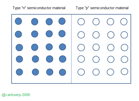
Figure 1. Schematic representation of the material type "n" and "p"
The free electrons will move from one end of the material to the other, that is, the electrons will travel towards the holes of the material "p", leaving behind if positive ions and at the same time creating negative ions of the other end (figure 2). This process continues until a region of positive ions forms in the material "n" and equally negative ions form in the material "n", but these do not continue indefinitely for two reasons:
When an electron tries to move towards the material "p", it is first attracted by the positive ions in region 1 and then repelled by the negative ions in region 2.
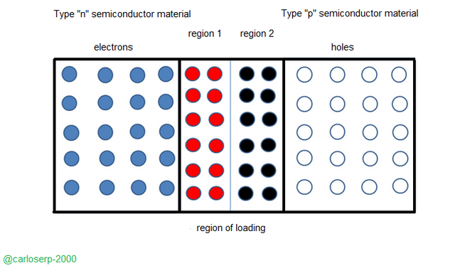
Figure 2. Schematic representation of the p-n junction in a materialemiconductor
However, after the region of charge reaches a certain thickness, the process of electron migration towards the end where the material "p" is located stops.
Now let's see what happens if we apply a difference of potential to the joint "p-n", as I mentioned before the electrons do not cross to the other end, because they are attracted by the positive ions and repelled by the negative ions, in order to jump from one end to the other and overcome the barrier they need an extra force that allows the electrons to jump over the barrier, and that is precisely what we get by a difference of potential.
If we connect to the material "p" then the electrons will be attracted to the end where the material "p" is, and if the potential difference is big enough the electrons will cross the barrier and an electric current will be created at the junction, this whole process is known as direct polarization.
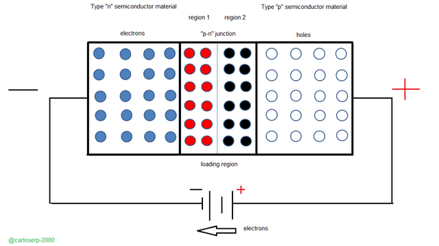
Figure 3. Direct polarization diagram
On the other hand, when the junction p-n is polarized in reverse, i.e. with the negative in the material "p" and the positive in the material "n", the electrons cannot flow from the end "n" to the end "p", on the contrary they are attracted towards the positive terminal, moving away from the region of charge, therefore there is no electrical conduction in this type of polarization, and this is the principle on which the diode is based, remembering that diodes conduct electricity when polarized in one direction and do not conduct electricity when polarized in the reverse direction.
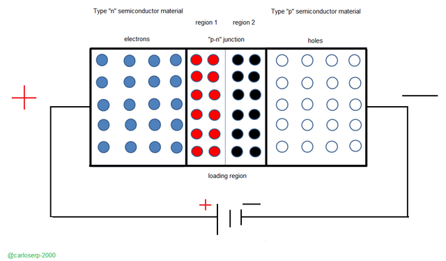
Figure 4. Reverse Polarization diagram
It is very important to know the physical process involved in determining a p-n junction in a semiconductor. This structure is fundamental for the creation of different optoelectronic devices as mentioned at the beginning of this publication. Diodes, transistors and solar cells are the main technological applications of this junction. Silicon was the main semiconductor compound studied to make this type of structure, since it has the physical capacity to become both materials (type p and n), so it was the first material that performs this function. After being so successful, the scientists decided to continue investigating and to create new materials that presented this behavior. At present we are working with several extrinsic and intrinsic materials to create new semiconductors.
Cover image sources:
If you want more information about the subject you can visit the following links:
Publish through our official app and you will get an extra vote of 5% https://www.steemstem.io/

 Video credits @gtg
Hi @carloserp-2000, thanks for sharing and explaining science with simple words. We need more authors doing that in the community.
Posted using Partiko Android
thanks for your words @ritch
This post has been voted on by the SteemSTEM curation team and voting trail. It is elligible for support from @utopian-io.
If you appreciate the work we are doing, then consider supporting our witness stem.witness. Additional witness support to the utopian-io witness would be appreciated as well.
For additional information please join us on the SteemSTEM discord and to get to know the rest of the community!
Thanks for having added @steemstem as a beneficiary to your post. This granted you a stronger support from SteemSTEM.
Thanks for having used the steemstem.io app. You got a stronger support!
Hi @carloserp-2000!
Your post was upvoted by Utopian.io in cooperation with @steemstem - supporting knowledge, innovation and technological advancement on the Steem Blockchain.
Contribute to Open Source with utopian.io
Learn how to contribute on our website and join the new open source economy.
Want to chat? Join the Utopian Community on Discord https://discord.gg/h52nFrV