Learn more about the characterization of materials, "Scanning electron microscopy" technique used for semiconductor compounds
Hello friends for this occasion I want to show you another type of characterization used in semiconductors, it is not a device in itself that is only used for semiconductor compounds, it is used in the whole technological field in different branches of science, it is a very used tool in the medical, chemical, geological, and biomedical fields, among others. but also it is very used by us the experimental physicists, since with this apparatus we can observe as in a very detailed way how these compounds are formed, their size, texture, relief, grain shape and composition. And what I'm talking about is the well-known technique of Scanning Electron Microscopy (SEM).
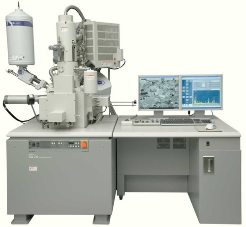
Figure 1. Scanning electron microscope.
Source
The operation of this equipment is based mostly on inciting a beam of electrons on the sample that we want to characterize, and by means of a screen we can visualize this information of the sample.
The SEM gives us an enlarged image of the upper part of the compound, each time the electrons impinge on the sample, the screen can enlarge up to 200,000 times the close image of the object, and that is why we can see up close how its texture on the surface of the same, this microscope has a resolution of 10nm and a depth of focus of 10mm, is much smaller than other microscopes this produces three-dimensional images of very high resolution.
Unlike other microscopes such as the optical and transmission, the SEM uses a beam of electrons instead of a beam of light to form the image, which is why currently is the most used to perform morphological studies and composition of materials.
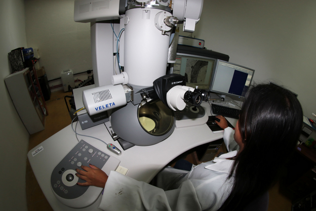
Figure 2. Model of equipment used in the IVIC.
Source
In Venezuela the scanning electron microscopy is practiced in the Venezuelan institute of scientific research (IVIC), and in other laboratories of different universities such as the University of Zulia, where I practice physics, and the Universidad de los Andes. In the facilities has a modern microscope in which investigations of character morfoligoco to different materials, the microscopy consists of the following parts:
*It presents a system to visualize the images, which would be the tube of cathode rays.
Vacuum system.
Refirgeration system.
Electric power system so that it can work correctly without power failure.
A program to record the images or photos of the compounds, this also records videos of the microstructure of the materials.
Sample shows, with a 360 degree turn to detect different angles of the materials.
Optical-electronic system, which generates the beam that moves on the sample of the material.
A system to detect the signals with the electron beam affect the sample, to then reflect the image of the materials to be characterized.
This equipment consists basically of one covered with a thin layer of carbon, this is done with the purpose that the device has electrical properties on the sample, that is to say, it is a conductor, followed by the scanning of the sample of the compound to be characterized , where the electrons are exited through a cannon, the detector measures is responsible for measuring the amount of electrons that affect the compound and similar to the X-ray diffraction equipment, this shows a record of intensities on the sample. From here finally I record all the data supplied in the equipment and we obtain a high quality image where we could observe by means of a micrograph the upper layer of the material.
Secondary detector:
This offers an image of the surface of the material in black and white, and gives a much more real image of said surface, is generated through the emission of valence electrons of the sample atoms, which in turn are excited and produce a topographic image of the surface of the material.
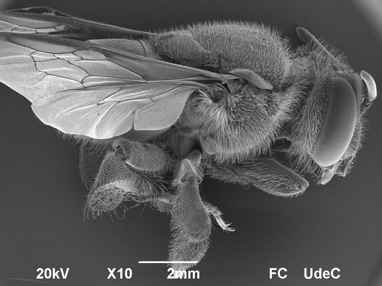
Figure 3. Micrography by means of secondary electrons.
Source
Detector of scattered retro electrons:
Unlike the secondary electron detector, it offers an image of the surface of the sample but with a lower resolution, it is formed by the electrons that leave the sample, this depends on the atomic number of the materials to be characterized, that is, the higher Atomic number of the material greater intensity.
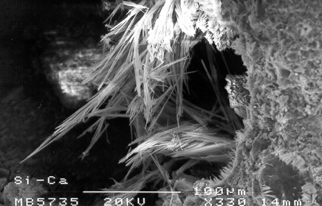
Figure 4. Ficrography by means of scattered retro electrons.
Source
As mentioned above, the SEM provides us with high-quality 3D images, images that provide us with information regarding the surface, topography and composition of the materials, for them the aforementioned detectors are used, all with a specific function depending on the material that you want to observe or characterize.
Its usefulness is very important because by means of them we can observe the morphology of the materials, how they were formed at the moment of being synthesized, they show unique characteristics of each material, for example in a semiconductor compound if we have the material and what we want to do with nanotubus, we can observe these nanotubes embedded in a very simple way by means of this device and that helps us to confirm that growth was done correctly.
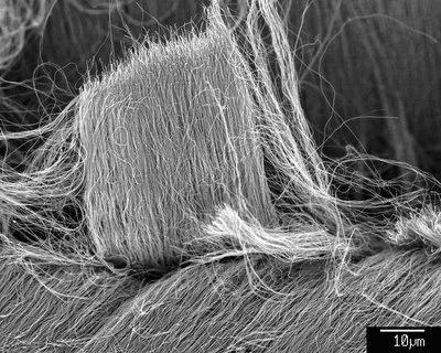
Figure 5. Carbon nanotubes.
Source
It is used for all types of characterization of materials such as:
Semiconductors, polymers, electronic devices, catalysts, food, wet materials and liquid materials, biological, in the oil and metallurgical engineering, biomaterials, drugs, botany and many more.
It helps to correctly identify the composition of the materieles, observe samples before preparing and see if it has any oxidation that may cause some damage in its growth, identify strange morphological compositions, behavior at the time of analyzing a sample because it is caused, combination of different detectors can amplify more images of the materials unlike optical microscopy or transmission.
Later I will continue explaining more about the world of semiconductors and their different types of characterizations, I hope the post has been to your liking. See you friends.
For more information about the subject visit the following pages
https://es.slideshare.net/vegabner/microscopia-electronica-de-barrido
https://www.ecured.cu/Microscopio_electr%C3%B3nico_de_barrido
http://www.nanocentro.ipn.mx/Servicios/Documents/MEB.pdf
http://www.laboratorios.bogota.unal.edu.co/vercontenido.php?idc=37
https://es.wikipedia.org/wiki/Microscopio_electr%C3%B3nico_de_barrido
Congratulations @carloserp-2000! You have completed some achievement on Steemit and have been rewarded with new badge(s) :
Click on any badge to view your own Board of Honor on SteemitBoard.
For more information about SteemitBoard, click here
If you no longer want to receive notifications, reply to this comment with the word
STOPThanks @steemitboard
Congratulations @carloserp-2000, this post is the most rewarded post (based on pending payouts) in the last 12 hours written by a User account holder (accounts that hold between 0.1 and 1.0 Mega Vests). The total number of posts by User account holders during this period was 2009 and the total pending payments to posts in this category was $1407.39. To see the full list of highest paid posts across all accounts categories, click here.
If you do not wish to receive these messages in future, please reply stop to this comment.
Thank you very much, I feel very happy
Excellent post @carloserp-2000. Congratulations!.
Regards!.
Thank you very much @tsoldovieri