Integrated Circuits: Fabrication and Classifications
Jack Kilby might be considered one of the greatest electrical engineers of all time for one invention; the integrated circuit. He went on to develop the first applications for this integrated circuits – including the first pocket calculator (pocketronic) and computer that used them.
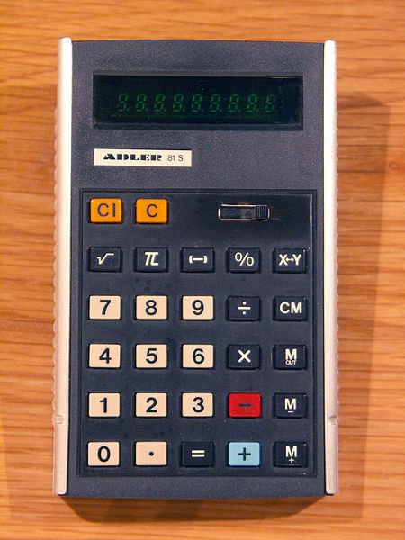
Pocket Calculator source: Wikimedia Commons - Public Domain License.
Electronic circuits have undergone tremendous changes since the invention of the triode by Lee De Forest in 1907. In those days, the active components like transistors and triodes and passive components like resistors and capacitors etc. of the circuits were separate units connected by wires and tie points.
The development of the transistor by W.H Brattain and I. Bardeen in 1948, the electronic circuits became considerably smaller in size. It was due to the fact that a transistor was not only cheaper and less power consuming but was also much smaller in size than its predecessor. To take advantage of the small transistor size, the passive components too were greatly reduced in size thereby making the entire circuit very small.
What is an integrated circuit?
An integrated circuit is an electronic circuit that is made up of small semiconductor devices and other electronic components that are manufactured from a semiconductor material most especially silicon. Open up a TV, a computer, a phone or even a radio and you’ll see it built around a printed circuit board, like an electric street map with small passive electronic components such as resistors, capacitors and inductors in place of the structures and printed copper connections linking them together like a street way. The basic idea of developing the integrated circuits was to make a large circuit, with all its complicated components and the connections between them, and recreate the whole thing in a tiny form on the surface of a piece of a semiconductor – silicon. It made possible all kind of electronic gadget, from pocket sized calculators, mobile phones, digital wristwatches, MP3 players, digital cameras, laptops to space-landing rockets with built-in satellite navigation control.
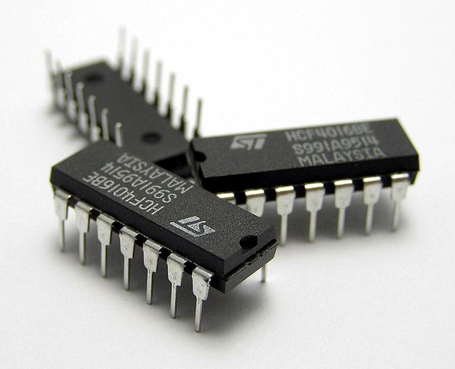
Integrated Circuits source: Wikimedia Commons - Public Domain License.
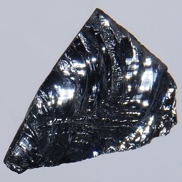
Raw material for fabricating an integrated circuit
pure silicon is the base for most integrated circuits. It is the substrate for the entire chip and it is chemically doped to make the P and N regions that make up the integrated circuit components. Silicon, as an element is not found in nature. However, it is found abundantly in nature in the form of silicon dioxide, which constitutes about 20% of earth crust. Silicon is commonly found as quartz or sand. A number of processes are required to convert sand into pure silicon with a crystalline structure. The sand is allowed to react with gas produced from the burning of carbon. This produces silicon with 98% purity. Next silicon is further purified in a reactor to produce electronic-grade crystalline silicon.
.jpg)
Pure Silicon source: Wikimedia Commons- Public Domain License.
.jpg)
Processes involved in fabricating an integrated circuit
- Wafer preparation: pure crystalline silicon is cut off into long cylinders and sliced into thin wafers.
- Masking: this process involves oxidation which consists of growing a thin film of silicon dioxide on the surface of a silicon wafer. Silicon dioxide as several uses:
i. To serve as a mask against implant or diffusion of dopant into silicon
ii. To provide surface passivation.
iii. To isolate one device form another
iv. To act as a component in metal oxide semiconductor structure. - Etching: is the process of selective removal of regions of semiconductor, metal or silicon dioxide. The wafers are immersed into a chemical solution at a predetermined temperature. In this process, materials to be etched is removed equally in all direction making a kind of pattern showing were n-type and p-type silicon are wanted.
- Doping: this process consists of introduction of impurities into selected regions of the wafer by heating it with gases to form n-type and p-type junctions of the silicon. More masking and etching may follow.
- Testing: after the wafer of the monolithic circuits has been processed and the final metallization pattern defined, it is placed in a holder under a microscope and is aligned for testing by a machine called multiple-point probe. The probe consists of contacts which are connected to the individual integrated circuit, and a series of tests are made to verify the electrical properties of the device in a very short time. Any chips that doesn’t work are marked and rejected.
- Packaging: the final step in integrated circuit fabrication is packaging the device in a suitable medium that can protect it from environment of its intended application, and ready for use in computers and other electronic equipment.
Classifications of integrated circuits
Integrated circuits can be classified based on the type of signals they process and these are:
- Analog integrated circuits: both the input and output signals in this types of ICs are continuous. The output signal depends strength on the input signal strength. Analog ICs are mostly used in power supplies, instrumentation and communications as in the case of audio frequency amplifier and radio frequency amplifier.
- Digital integrated circuits: these ICs operates with discrete signal such as 0 and 1. Digital ICs includes logic circuits such as AND gate, OR gate, NAND gate, flip flops, microprocessors and microcontrollers. Digital ICs are used in computers, cellular phones and televisions.
- Mixed-signals integrated circuits: these ICs converts digital signals to analog signals, which can be used to control the speed of motors, the brightness of lights and the temperature of heaters. Mixed-signals ICs can also convert analog signals to digital signal.
Advantages of integrated circuits
i. Extremely small physical size
ii. Very small weight
iii. Reduced cost
iv. Extreme high reliability
v. Increased response time and speed
vi. Low power consumption
vii. Easy replacement
viii. Higher yield
Disadvantages of integrated circuits
i. Coils or inductors cannot be fabricated
ii. Integrated Circuits function at very low voltages
iii. They can handle only limited amount of power
iv. They are quite delicate and cannot withstand rough handling or excessive heat.
Conclusion
As it can be seen that the advantage of integrated circuits far outweighs their disadvantages. The applications of Integrated Circuits are numerous. One of the widely accepted application is in mobile phones and computer systems. Another application is the electronic calculator which can perform various functions like addition, subtraction, multiplication and division. There are also advanced scientific calculators that are programmable and can display graphs.
References
- Explain that stuff
- Electrical Engineering Stack Exchange
- Electrical Technology
- Brighthub Engineering
- Electrical4u
- Sciencing
If you write STEM (Science, Technology, Engineering, and Mathematics) related posts, consider joining #steemSTEM on steemit chat or discord here. If you are from Nigeria, you may want to include the #stemng tag in your post. You can visit this blog by @stemng for more details. 
So an audio amplifier falls under which example of integrated circuit?
A layman asking.
An Audio amplifier is not an integrated circuit.
However, you find numerous integrated circuits in modern Audio amplifiers.
Thank you.
Nice piece @doctorchungs. Semi-conductors are indeed one important class of materials with fascinating applications.
Keep steeming!
Thanks @temitayo-pelumi
Interesting article you've got here mate. Silicon mostly plays a vital role in semi conductors. It is also use to make CMOS (complementary metal oxide semi conductors) batteries..I don't know if i am right?
From an electrical point of view. Keep it up bro
Yes, you're right... The CMOS is an integrated circuit design that also uses the semiconductor technology.
The invention of integrated circuit definitely turned the world around regarding gadgets and electronics in general. Nice piece @doctorchungs
I tell you... Thanks
A doctor and an engineer.. Great piece, just like led the material for integrated circuit Is silicon and it also has the p and N diode... Nice
Congratulations @doctorchungs! You have completed some achievement on Steemit and have been rewarded with new badge(s) :
Click on the badge to view your Board of Honor.
If you no longer want to receive notifications, reply to this comment with the word
STOPGreat piece. Really nice working going there.pcb manufacture : pcb companies