Do you know semiconductors? your answer is no... "I will explain to you very easily" Part # 3
In the previous publications I show you what a semiconductor means and what are the existing semiconductors, ie the two types of semiconductors, also tell you about the concentration of charge carriers inside them.
Now I would like to continue along the same lines, this time writing a little about the union of a p-type semiconductor and n-type semiconductor; essential junction for most of its applications in the area of technology for the manufacture of diodes, transistors and solar panels.
We would ask ourselves the following question. How would we make this union p-n?
And the first thing that comes to mind to answer this question would be:
We would simply perform this union by attaching a semiconductor material n to another p. If it is easy, but it turns out that it is not so, in addition to being in contact with each other physically, we must also know that they must be in electronic contact that would be essential for the construction of different electronic devices.
Logically, as we said before, the sum of the charges of the two crystals, before the union, will be neutral.
To summarize what has already been discussed in previous publications. zone n we have free electrons and in the zone p we have holes waiting to be filled by electrons.
Now the union p-n is that which is created by putting in contact a semiconductor n with a semiconductor p. When two p-type and n-type materials are placed in contact with each other, the union behaves very differently than would each of the materials separately.
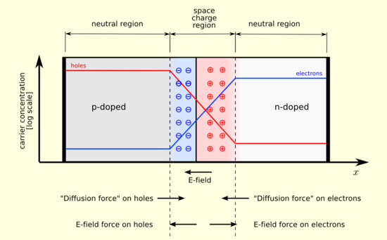
Figure 1. Diagram the p-n junction of a semiconductor.
Specifically when a direct polarized current is applied, ie a current flowing from a negative terminal to a positive terminal, the electrons flow using the available electrons and holes in both semiconductors, so that a continuous current is maintained in the flux of electrons.
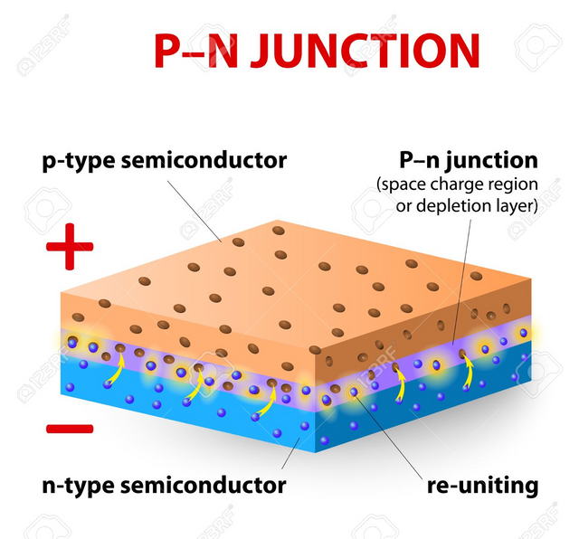
Figure 2. p-n junction.
In contrast, when a reverse polarization is applied, ie a current where the electrons flow from a positive to a negative terminal, the electrons tend to occupy first occupy the available holes in the p-type semiconductor; but once all the holes are occupied, the electrons will begin to repel each other, forming an area where there is no more flow of free electrons.
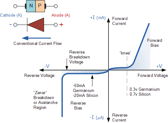
Figure 3. Characteristic curve of a semiconductor diode.
In summary:
Direct Polarization
Apply a Potential Difference (v), the p with term + and n with term -. Potential difference decreases (V_0-V) and that allows a greater I to the right.
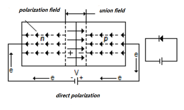
Figure 4. Diagram of the operation of a semiconductor diode when a voltage is applied to produce a direct polarization.
Reverse Polarization
Applies Potential difference (v) with p attached to terminal - and n with +. The potential difference increases now (V_0 + V) and this reduces the value of the Intensity.
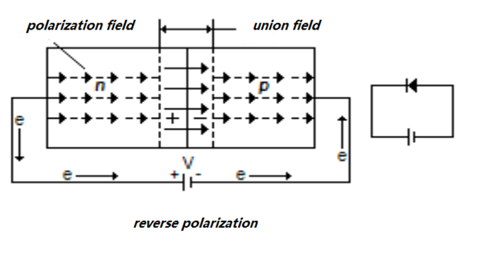
Figure 5. Diagram of the operation of a semiconductor diode when a voltage is applied that causes a reverse polarization.
For more information visit these pages:
- http://www.areatecnologia.com/electronica/union-pn.html
- https://www.123rf.com/photo_21930713_p-n-junction-p-type-silicon-layer-contains-more-positive-charges-called-holes-and-the-n-type-silicon.html
- http://www.circuitstoday.com/understanding-the-pn-junction
- http://www.electronics-tutorials.ws/diode/diode_3.html
- http://depa.fquim.unam.mx/amyd/archivero/condsemicondais2_27505.pdf
- http://depa.fquim.unam.mx/amyd/archivero/condsemicondais2_27505.pdf
Congratulations @carloserp-2000, this post is the third most rewarded post (based on pending payouts) in the last 12 hours written by a Dust account holder (accounts that hold between 0 and 0.01 Mega Vests). The total number of posts by Dust account holders during this period was 2442 and the total pending payments to posts in this category was $591.20. To see the full list of highest paid posts across all accounts categories, click here.
If you do not wish to receive these messages in future, please reply stop to this comment.
great work, amazing post
Thank you @brow10