New toy! Scanning Electron Microscope!!!
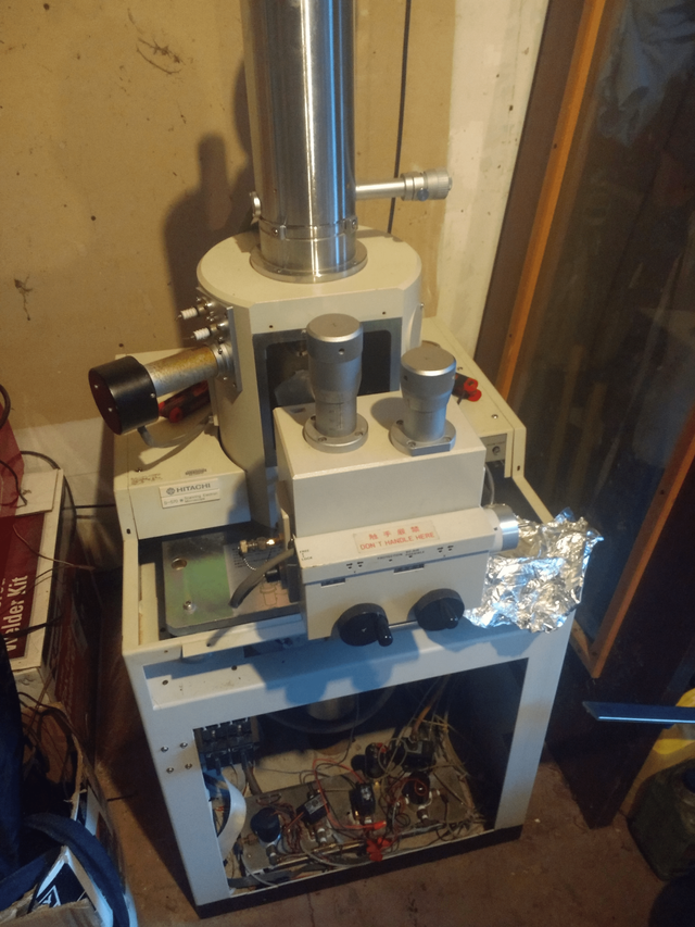
Figure 1. Hitachi S-570 Scanning Electron Microscope (SEM)
As the title suggests, I have recently been fortunate enough to purchase an old, non-functioning (for now) scanning electron microscope (SEM) for an unbelievable bargain from a university surplus equipment auction. For those who are unfamiliar with SEMs, they are used to take microscopic images in the micrometer and, for some more modern models, the nanometer range. SEM images can tell a great deal of information about a material's surface properties and and crystal structure, something that is heavily used in the material science field. Not only can they take images, but if the appropriate attachments are added, they can also perform Energy Dispersive X-ray Spectroscopy (EDS). EDS is a very important tool in the material science field because in addition to the SEM images, elemental analysis can be performed on the images which can give you a very good idea what a material might be composed of. There are other uses for SEMs, but these are the two that I am primarily interested in. Even if I am unable to get the SEM to function properly, I can reconfigure it to operate as an electron beam welder or as a powder bed electron beam based additive manufacturing system (think metal 3-d printer).
The electron microscope I have purchased did not come with any control software or computer. I will have to design and build much of this myself and plan on releasing the end-product as an open source hardware package for those looking to build or obtain their own SEM.
Below are various images of the SEM and components.
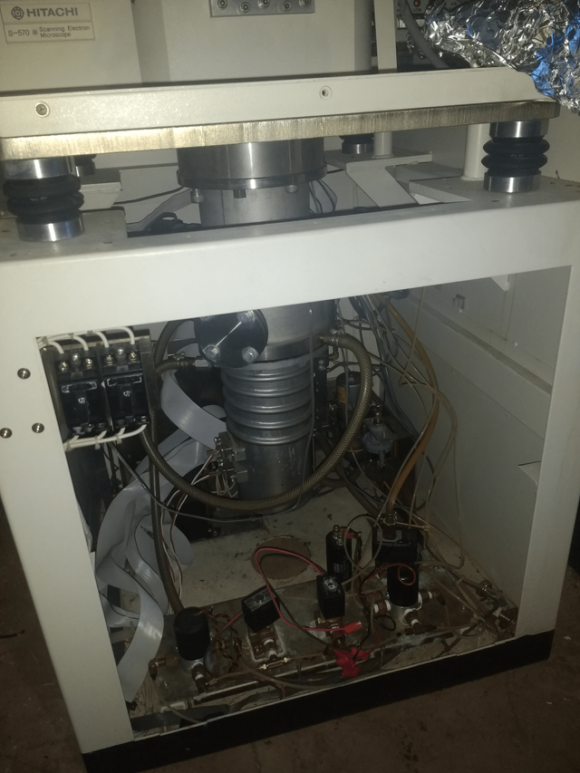
Figure 2. The diffusion pump, gate valve, and additional control hardware.
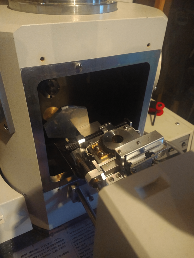
Figure 3. The sample stage and chamber.
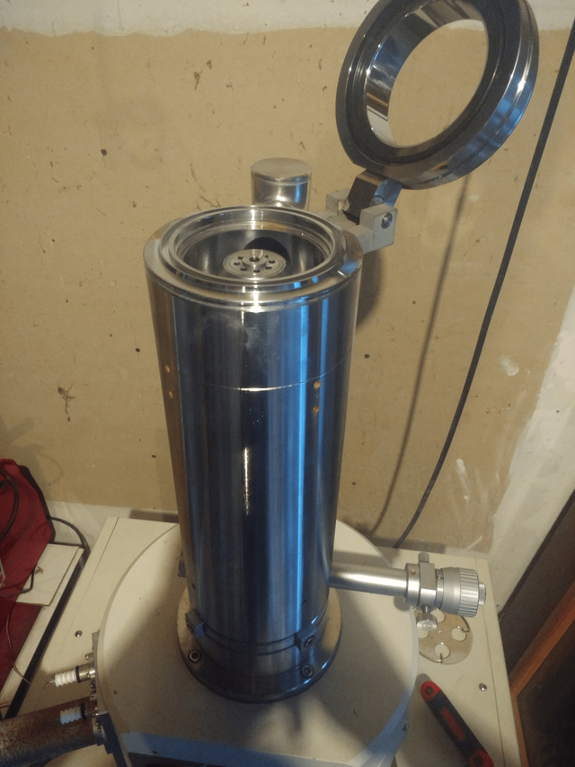
Figure 4. Electron column (electron source/gun goes on top where the flange is hinged).
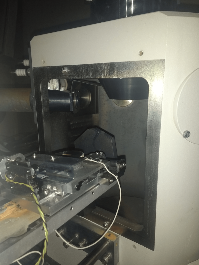
Figure 5. View inside the sample chamber as well as the backscatter detector sticking through the wall.
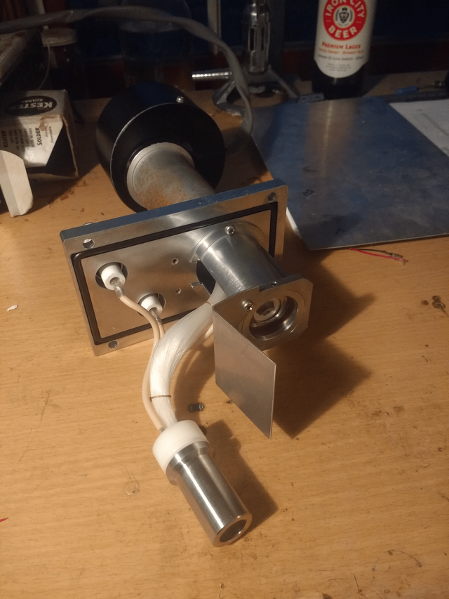
Figure 6. Backscatter detector removed from microscope column. The scintillation material was damaged at some point (white stuff in top part) and will need to be repaired.
As I work on this project I will post updates but will keep them more concise than my typical posts.
This post has been voted on by the SteemSTEM curation team and voting trail in collaboration with @curie.
If you appreciate the work we are doing then consider voting both projects for witness by selecting stem.witness and curie!
For additional information please join us on the SteemSTEM discord and to get to know the rest of the community!
Great you can buy this wonderful team, I have no doubt that you can do amazing things with the ... What kind of studies do you plan to do with the SEM?
Congratulations @hellfire-labs! You have received a personal award!
Click on the badge to view your Board of Honor.
Do not miss the last post from @steemitboard: