Do It Yourself : An Engineering Way to do the Etching process.
PCB / Circuitry Designing is part of the Engineering life. Though not all branch of Engineering is capable to do so since it is all about the majors. Electrical, Computer and Electronics Engineering (as far as i know) are the primary majors in Engineering which deals with the circuit designing. Furthermore, it is essential for these Engineers to be fully equipped with the skills to do the one of the fundamentals in printed circuit board printing & designing - the Etching process.
What is ETCHING?
A lot of you may be asking what is etching mostly to those non-engineering people. So , what is Etching?
It was Daniel Hopfer who was believe to be the first to apply this way of printmaking.
Etching is a process on designing a circuit on a metal plate which is usually covered by copper (common) , zinc or steel. It uses the strong acid mostly used today to those who just make it at home for project purposes is the Ferric Chloride (FeCl3). Furthermore, this can be also define as the process of dissolving the copper which is not covered by the protected layer.
Though some people prefer to use the UV Exposure box for an instant and precise etching yet too complicated for home based projects.
Hold On and We are going on a complete ride of DO IT YOURSELF!
Materials and Components Needed
The following should be prepared first before we proceed on the proper process:
• Acetate/Magazine/Sticker Paper(glossy)
• Ferric Chloride / Iron (III) Chloride
• Plastic Container
• Permanent Marker
• Sandpaper
• Circuit Design
the above images were arranged accordingly with the abovementioned.
ETCHING process : Step-By-Step
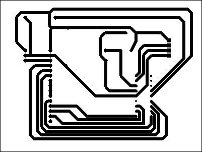
Step 1 : Design your circuit
- On this step, you need to have your design for your board. You may use software on Circuit Designing like Proteus, PCBWeb Designer, Fritzing and any other PCB Design Software.
Step 2 : Print out the design on a selected medium and Prepare the copper plate
- On this step, print out the desired design of the group into a selected medium like acetate paper, glossy sticker paper, magazine or any paper that have a shiny part on it. Why do we have to consider the shiny part? For an easy way to transfer the printed design on your copper plate. (In this case, we are using the acetate paper and please use a printed which uses a toner for an ink cartridge or laserjet.)
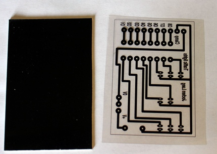
- Next is to prepare the copper plate. Rub the sand paper on the copper side of your copper plate. On this step, we are enabling the design which was printed on the acetate to stick on the copper when heated or transferred. Moreover, wash the copper plate with water and/or rubbing alcohol. Let it dry for a few minutes.
Step 3 : Putting the design to the copper plate and prepare for the heating process.
Cut out your design and put it on the copper side of the copper plate facing down. (Tip: you may put a paper tape so that the paper would not move during the heating process)
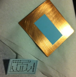
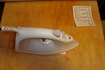
Run the iron above the copper plate with the design being attached to the copper. (Tip: put the intensity of the iron to the maximum for a quicker method) Wait for quite some time preferably 30-45 minutes. T. If you have laminator , you may use it instead.
Step 4 : Separating the paper from the copper plate.
- Soak the copper plate together with the attached paper to a water and then slowly remove the paper from the copper plate.
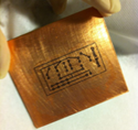
the result : the design already transferred to the copper plate
Step 5 : Main etching process
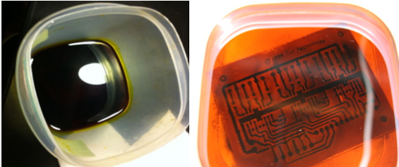
- This is the main process in which the Printed Circuit Board (referring to the copper plate with the design being transferred through the heating process) will be soaked to the etching solution which can be a Ferric Chloride. Placed the PCB on the Ferric Chloride and be sure to soak it properly most especially on the copper side. This process will dissolve the copper which was not covered / protected by the printed area.
Step 6 : Finishing touches . . .
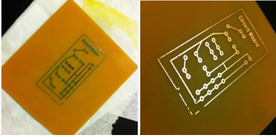
- When the unnecessary copper area is totally washed out, rinse it with water and let it dry. (you may rub an alcohol for the finishing touches also)
FURTHER NOTES
- Dispose properly the etching solution, it is a hazardous material. And do not pour it down on the drain since it may eat up your pipes. AND it is also toxic.
- After the etching process then you will proceed to the drilling method. Tips: use a dremel, a 1/32 inch drill bit.
This is an Engineering DIY post. You may comment down and ask for more DIY topics, be more than happy to post it for you :D
ENJOY AND HAVE A GREAT LIFE AHEAD
Bidding a goodbye, See you then :)


Your post is very interesting.
your post resteemed!
@mdo Thank you so much :) I hope to have more Do It Yourself posts that can be helpful for other steemians.
Steem On!
nice post
Thank you for that commendation. Steem On!
Damnn, this was a really cool post....;-)
Thank You so much. It is heartwarming to know that I can help someone from this post.
Congratulations @leryam12, this post is the most rewarded post (based on pending payouts) in the last 12 hours written by a Newbie account holder (accounts that hold between 0.01 and 0.1 Mega Vests). The total number of posts by newbie account holders during this period was 2628 and the total pending payments to posts in this category was $1196.54. To see the full list of highest paid posts across all accounts categories, click here.
If you do not wish to receive these messages in future, please reply stop to this comment.
Congratulations, your post received one of the top 10 most powerful upvotes in the last 12 hours. You received an upvote from @curie valued at 42.63 SBD, based on the pending payout at the time the data was extracted.
If you do not wish to receive these messages in future, reply with the word "stop".
Hello @leryam12u !
Your posts are very interesting, you can follow me, I have civil engineering posts, you can see them.
Greetings 😊